

Research
- Silicon Photonics
- Space Weathering
- Defects in Semiconductors
- Positron Annihilation Spectroscopy
- Research Opportunities
- Publications
Contact Information
Prof. Peter Simpson
Physics & Astronomy 210
(519) 661-3390
psimpson [at] uwo [dot]ca
FAX: (519) 661-2033
Defects in Semiconductors
A problem of current interest in physics is how to design, produce, and characterize nanometer-scale functional structures. It is expected that this will eventually impact microelectronics, telecommunications and information networks, computer technology, and advanced materials and manufacturing.
Point defects (vacancies, i.e. atoms missing from the crystal structure, and impurities) determine the electronic properties of materials used for integrated circuits. To develop new materials and processes, an understanding of defect structures and behaviour is vital, and will become more so in the future as devices are made smaller and faster.
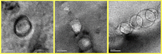
Defect engineering exploits the properties of vacancy-type defects to achieve materials properties that are not naturally occurring. For example there has been considerable interest in recent years in the formation of voids in silicon, to act as gettering centres for impurities, or for sectioning technologies. Void formation proceeds by ion implantation of gases such as He and H followed by thermal annealing. Vacancy-type defects introduced by implantation are stabilized by the implanted gas atoms, and coalesce to form voids. Besides the technological applications, there is considerable interest in understanding the underlying physics of these processes.