


Research
- Research Overview
- Organo Metallic Chemical Vapor Deposition
- Optical Response of Gold Nanoparticle Clusters
- Evanescent Wave Analytical Tools
- Surface Functionalisation
- Detection of Optically Active Molecules
- Optical Tweezers in Evanescent Fields
- Evanescent Microscopy and Spectroscopy
- Research Opportunities
- Research Group
- Former Coworkers and Students
- Collaborators
- Publications
Contact Information
Prof. Silvia Mittler
Physics & Astronomy 240
(519) 661-2111 x.88592
smittler@uwo.ca
FAX: (519) 661-2033
Evanescent Wave Analytical Tools
These techniques are the fundament of the photonic work done in the group. The evanescent fields of waveguide modes and surface plasmon resonances are used to detect changes right within these fields. Therefore very often the sample of interest is located on top of a waveguide or on top of a gold layer there where these evanescent fields are present. Changes which can be detected by theses "films of light" are typically optical changes: refractive index, absorption coefficients and thickness. Any treatment of a material which changes one of the previously mentioned optical qualities can therefore be also monitored. For example: Adsorption processes of any kind to the waveguide surface or to the gold surface: both physisorption and chemisorption processes, photo bleaching reactions, where the refractive index of the material is changed, thermal expansion of material, etc.
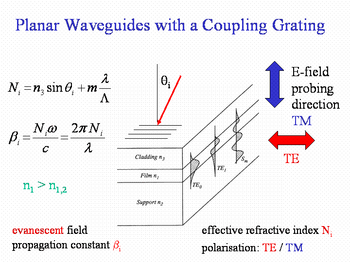
A scheme of a planar waveguide carrying a coupling grating is shown. The refractive index of the waveguiding layer has to be higher than the refractive indices of the surrounding materials to assure a total internal reflection and a guiding of the light within this particular film. There are specific resonances where such a guiding takes place. Having a close look to the field distribution of the electrical field in the resonance cases one finds a standing wave across the structure with evanescent fields both located in the cladding and the substrate. These resonances can be excited in two polarisation directions, denoted TE-modes for s-polarised light and TM-modes for p-polarised light. Therefore a probing of the waveguide film itself and of material located on top can be done out-of-plane and in-plane by choosing the proper polarisation condition. Also each individual mode has its own propagation constant (beta) or effective refractive index N. These numbers can be measured by measuring the resonant coupling angle theta for each mode and plug it into the equation for N. Here one must know the periodicity of the coupling grating (capital lambda), the coupling order (m) and the wavelength of the used light (small lambda). By measuring more than one mode in both polarisation directions, it is possible to calculate the thickness and both refractive indices of of an adlayer or the waveguide itself. Anisotropic changes can be monitored by this method as well.
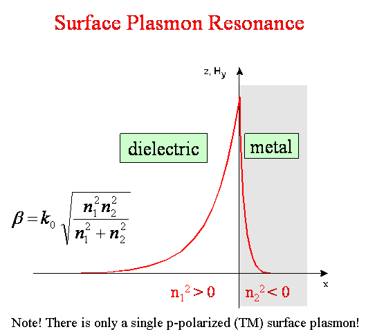
In the case of a surface plasmon resonance not a guiding film is necessary, but a metal-dielectric interface typically located on a substrate for handling purposes. In this geometry only one resonance excists. Therefore one needs to know more details about the system under consideration to measure specific quantities. Neverthless the strength of the evanescent field in the case of a surface plasmon is larger than for waveguide modes. Therefore the sensitivity is typically larger with surface plasmon resonances in comparison to waveguide modes. Also a surafce plasmon is a guided wave. It also has a propagation constant beta. The energy is not carried very far, because the metal dissipates it in about one micrometer.

A combination of surface plasmons and waveguide modes is possible. This allows to independetly determine the out-of-plane refractive index and the film thickness of material located on a metal.
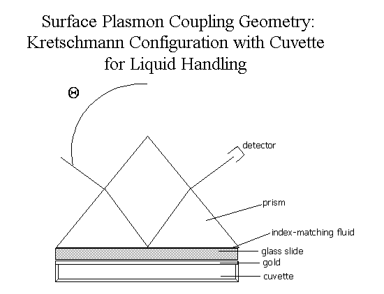
Detail of the prism - gold sample geometry in Kretschmann configuration with a cuvette for fluid sample handling.
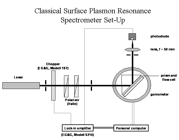
The entire set-up for surface plasmon resonance spectroscopy. Laser light in p-polarisation attenuated to a defined intensity is incident on the prism-sample mount. The prism-sample mount is located on a turning stage in order to change the incident angle theta. The back refelcted light is collected via a lens and a detector unit under two theta.
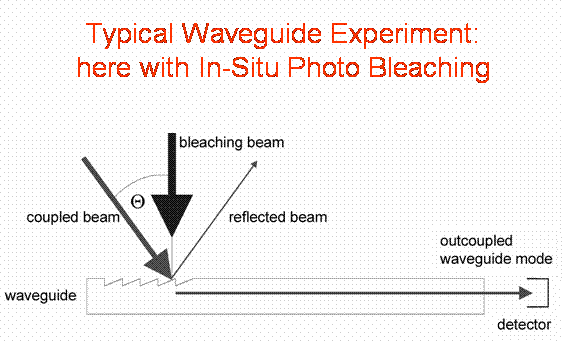
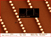
Typical waveguide set-up: the angle of incidence theta is scanned from left to right across zero degree angle of incidence by a goniometer and monitoring the out-coupled intensities, basically at both ends of the sample. Here just one side is shown. In this particular example a bleaching beam is present, which does a photo reactioin within the waveguide material. So by measuring the coupling angles with increasing bleaching time the photo reaction can be monitored, because it changes the optical constants of the waveguide.
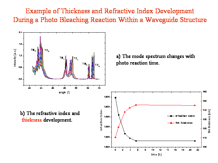
Waveguide mode spectrum development with bleaching time and the corresponding data analysis of the refractive index and the film thickness of the bleached waveguide material. The example here shows a material which shows an increase in film thickness due to the photo reaction. This is due to an increase of space needed on the molecular level. On the other hand with this volume incraese a density decrease is occuring, which is represented in the decrease of the refractive index. (data from Bernhard Menges and Alexander Theis)
